Last Updated: 15 June 1995 The SVT is made of 216 silicon detectors . The silicon drift detector operates in a manner analogous to gas drift detectors. Fig. 1 shows a schematic layout that illustrates the geometry and operation of semi-conductor based drift chambers.
A 4 inch, high resistivity (around 3 K /cm) n-type Si wafer
is used as a substrate.
Field
shaping electrodes are constituted of p-type material implanted
symmetrically on both surfaces in a regular strip pattern. The pitch
between cathodes in the STAR SDD prototypes is 120
/cm) n-type Si wafer
is used as a substrate.
Field
shaping electrodes are constituted of p-type material implanted
symmetrically on both surfaces in a regular strip pattern. The pitch
between cathodes in the STAR SDD prototypes is 120  m. A high voltage
gradient (up to 600 V/cm) applied to these shaping electrodes fully
depletes the Si thus creating a deep potential well that attracts free
electrons produced by the passage of charged particles through the detector.
The surface electrodes are
symmetrically connected to a voltage divider network that produces an
independent electrostatic field parallel to the surface of the wafer.
The field transports the electrons towards the edge of the detector
where signals are read out on a segmented anode (pitch = 250
m. A high voltage
gradient (up to 600 V/cm) applied to these shaping electrodes fully
depletes the Si thus creating a deep potential well that attracts free
electrons produced by the passage of charged particles through the detector.
The surface electrodes are
symmetrically connected to a voltage divider network that produces an
independent electrostatic field parallel to the surface of the wafer.
The field transports the electrons towards the edge of the detector
where signals are read out on a segmented anode (pitch = 250  m).
Under suitable conditions,
the electron drift velocity is constant, so that a measure of the drift time
is equivalent to a measurement of the position in the drift direction.
During drift, with typical speed of 1
m).
Under suitable conditions,
the electron drift velocity is constant, so that a measure of the drift time
is equivalent to a measurement of the position in the drift direction.
During drift, with typical speed of 1  , the initial cloud of
electrons expands due to diffusion and Coulomb repulsion. The charge thus
read out is shared among few anodes (2-6) over a somewhat extended time
period (few 100 ns).
Charge sharing techniques can then be used to determine the
original position of the cloud to an accuracy better than the anode pitch.
Prototypes of this technology were used in the CERN NA45 (CERES) experiment
and have been found to have excellent position sensing precision and
resolution (< 10 microns). This remarkable
position resolution can be achieved at a small fraction of the cost
associated with a pixel detector of equivalent resolution.
, the initial cloud of
electrons expands due to diffusion and Coulomb repulsion. The charge thus
read out is shared among few anodes (2-6) over a somewhat extended time
period (few 100 ns).
Charge sharing techniques can then be used to determine the
original position of the cloud to an accuracy better than the anode pitch.
Prototypes of this technology were used in the CERN NA45 (CERES) experiment
and have been found to have excellent position sensing precision and
resolution (< 10 microns). This remarkable
position resolution can be achieved at a small fraction of the cost
associated with a pixel detector of equivalent resolution.
The SVT drift detectors are based on the above model. Prototypes are currently designed and fabricated at BNL. A bi-directional drift detector with minimized guard area ('mini guards') will be used in the final SVT design to allow operation with a maximized active area at a reduced voltage.
Table II gives the specifications and critical parameters for the Silicon Drift Detectors to be used for the SVT.

Figure: Functional diagram of generic n-type Silicon drift detector
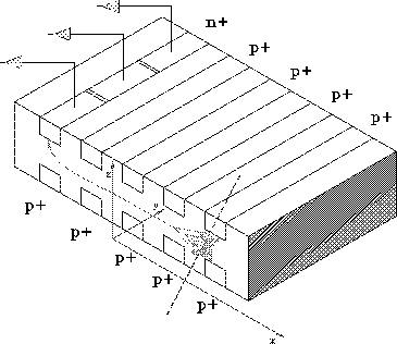
Table: SDD specification and critical parameters