Requirement:
The DAQ system will be able to probe and verify the presence and geographical ID of all RDO systems of the SVT.
Justification:
Correct DAQ system operation requires an exact understanding of the connection of the RDO systems to the SVT. An automatic probe and verifcation of the geographical location of each SVT RDO system is required to provide this information in a concise and reliable manner. This capability is essential to identify errors resulting from incorrect connection of fibers carrying the detector raw data stream.
Figure 2 shows a top level view of the TPC and SVT DAQ system and how they are connected to each other.

Figure: An overview of the TPC and SVT data
acquisition system
The SVT DAQ system is similar in structure to the TPC DAQ system and processes the SVT data in parallel to the TPC data. The first time the TPC and SVT data are combined is at the time of the global level-3 trigger decission and at the event builder level via the level-3 backbone network. The SVT will contribute a set of logic flags to the global level-3 decission CPU, which are combined with the logic flags from the TPC and other detectors.
The whole SVT detector is divided into 8 logical sectors, which are processed in parallel in the DAQ in separate logical "sector crates". Each sector crate will contain 3 receiver boards for the 3 fibers of the readout systems in each sector, plus an undetermined number of level-3 processors (depending on the processor power needed for the SVT level-3 algorithms). Each sector crate will also contain a 68040 based "housekeeping" processor board to manage booting and configuration of the other CPU's in the crate, plus a bridge to the level-3 backbone network (this can possibly be accomplished by the housekeeping processor, if the choice of the level-3 trigger backbone network allows this).
Due to budget constraints 2 logical sector crates will be combined in one physical VME crate, sharing the housekeeping processor and network bridges. Figure 3 shows one of 4 SVT sector crates.
The level-3 processors will be off-the-shelf RISC processor boards. The choice of the specific processor will be delayed as late as possible in order to get the most processing power for the alloted budget. The only requirements on these processor boards are that they are available with the appropriate network connection (currently, the choice for the sector crate network is VME64), and that they provide the necessary software developement environment to port the level-3 algorithms to them (probably some Unix derivative or a realtime operating system). These processors will be supported by the DAQ group.
The receiver boards in the sector crates are custom built by the DAQ group and provide for the level-3 pre-processing, i.e. cluster and space point finding. Figure 4 shows the information entering and leaving the receiver card.
Each receiver card will receive data from one readout system via the HP Gigalink fiber, and provide space point summary information for all 18 detector halfs serviced by the readout systems to the level-3 CPU's. In addition each receiver card has interfaces to trigger and to the event builder(s), plus capabilities to configure it and exchange the tables needed for level-3 pre-processing. Figure 5 shows a top-level view of one of the 24 SVT receiver cards.
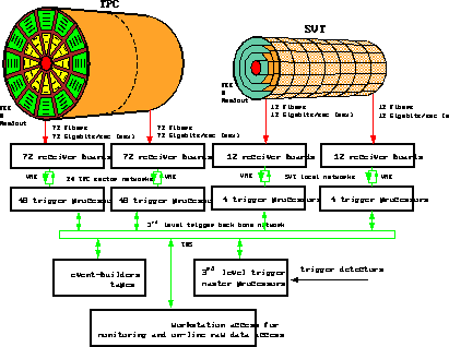
Figure: Sketch of one of 4 SVT sector crates
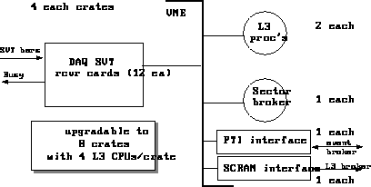
Figure: The interfaces of the receiver board
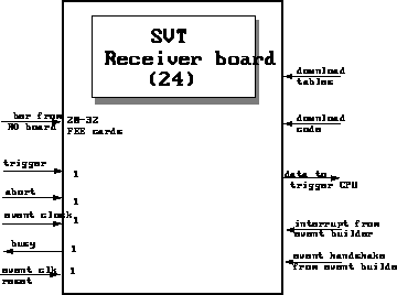
Figure: Top level of the receiver card used for TPC and SVT
Each receiver card consists of a mother board which houses 3 identical mezzanine cards. The mother board contains the Gigalink receiver logic and deserializer plus demultiplexing circuitry to distribute the raw data to the 3 mezzanine cards. The three mezzanine cards will be connected to the mother board via a global bus. Currently, this global bus is chosen to be a PCI bus with PMC style connectors. The PCI bus provides the connection to the VME64 backplane via a PCI-VME64 bridge chip. Additionally, the PCI bus will provide access to a global RAM on the mother board, which can be used to store the space point information. The hardware to accomplish the level-3 preprocessing itself is contained on the mezzanine cards.
The details of the Gigalink receiving logic on the mother board are shown in Figure 6.
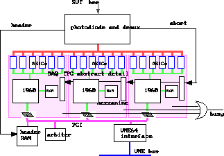
Figure: Details of the receiving logic
on the receiver mother board
The Gigalink fiber from the readout system is connected to the Gigalink photodetector. The output of the photodetector is connected to the deserializer chip which provides the received data on a 20-bit bus. This 20 bit bus is split into 2 separate paths. One of these paths leads to a separate storage for the header information (possibly just a FIFO), which makes the header information available to the PCI bus for later retrieval. The other part of the bus is connected to a demultiplexing logic. The demux splits the 20-bit data words into two 10-bit data paths and strobes these 10-bit data words into 9 ASIC's for each 10-bit path. The ASIC's are addressed sequentially via the data strobes to reduce the write rate into each individual ASIC to 1/9th of the incoming Gigalink rate.
One of three mezzanine cards of a receiver board is shown in Figure 7.
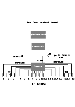
Figure: One of 3 mezzanine cards of the receiver board containing the ASIC's and the i960 for level-3 pre-processing
The
mezzanine cards are the actual workhorses to accomplish the level-3
preprocessing. Each mezzanine card contains 6 ASIC's and one embedded RISC
processor (currently, the choice for the RISC processor is the Intel 80960,
the "i960"). The ASIC's do the first stage of the level-3 proe-processing.
Each ASIC will receive the complete raw data from one detector Hybrid (1/2 of
an SDD). For each 10-bit data word the ASIC will subtract an 8-bit
pedestal value (stored in an external SRAM and addressed by the ASIC via the
sum of the time index plus a pedestal offset delivered in the event header),
and then convert the 10-bit value to an 8-bit value via an external lookup
table (also stored in the external SRAM). The storage requirement for the
pedestal values is: 256 anodes 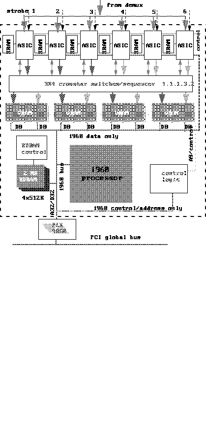 128 timebuckets = 32 kB. To store the
translation lookup table we need: 256 anodes
128 timebuckets = 32 kB. To store the
translation lookup table we need: 256 anodes  1024 lookup-values = 256 kB
(the number 256 arises, because this lookup table also allows for
anode-by-anode gain corrections by changing the lookup values for each anode
appropriately). Therefore the total size of the external SRAM attached to each
ASIC has to be at least 278 kB, which will require 3 external chips (128 kB
each).
1024 lookup-values = 256 kB
(the number 256 arises, because this lookup table also allows for
anode-by-anode gain corrections by changing the lookup values for each anode
appropriately). Therefore the total size of the external SRAM attached to each
ASIC has to be at least 278 kB, which will require 3 external chips (128 kB
each).
As the ADC data are being acquired 256 cluster pointer lists are being compiled: Each ADC value, after translation is compared with a common threshold value, THRESH_LO. Clusters are defined as sequences of consecutive timebins (for a single anode) whose translated values exceed the threshold. A qualifier, N_SEQ_LO, is used to specify that only sequences of N_SEQ_LO+1 timebins above threshold define a cluster. A second threshold, N_SEQ_HI, and associated qualifier, N_SEQ_HI, are used to further qualify the cluster before it is included in the cluster list. For this second threshold, N_SEQ_HI+1 timebins (not necessarily consecutive) must exceed THRESH_HI, during the interval in which N_SEQ_LO is being satisfied.
For sequences which meet both criteria, the beginning of a sequence t is
defined as the number of the first timebin to exceed TRESH_LO, or timebin 0
when its value exceeds the threshold value. The end of a sequence t
is
defined as the number of the first timebin to exceed TRESH_LO, or timebin 0
when its value exceeds the threshold value. The end of a sequence t is
defined as the number of the timebin whose translated value exceeds the
threshold, but the following value does not, or timebin MAX_TIMEBIN, provided
its value exceeds the threshold.
is
defined as the number of the timebin whose translated value exceeds the
threshold, but the following value does not, or timebin MAX_TIMEBIN, provided
its value exceeds the threshold.
The cluster RAM stores 256 lists; each list is composed of up to 8 pairs of 10-bit numbers, representing the first and last timebin in a qualifying sequence. Once the capacity of the anode (8 clusters total per anode) is reached, no further data are written to the cluster RAM for this anode.
The output of this procedure as well as the translated ADC values are stored in 8 VRAM chips via 2 3x4 crossbar switches (The number of VRAMs can be increased to allow for more events to be stored in the receiver cards). Currently, these VRAM's provide for storage of up to 7 events on the receiver cards.
The VRAM's are also connected to a bus that is accessable by the i960 on the mezzanine card. A program running in the i960 will use the information stored in the cluster-pointers and the (translated) ADC values to compile 2-dimensional clusters. It will then use a simple moment analysis to extract the centroids of these 2-dimensional clusters, a measure of the total charge of a cluster, and a measure for deciding if the cluster resulted from a single or many particles traversing the SDD. The centroid will be used as the space point for this particle crossing and will be stored in the global RAM to be passed on to the level-3 processor(s) for further processing (tracking).
The 2MB EDRAM associated with each i960 will be used to store a program and data memory for the i960. This memory will be made accessable via the VME bus to assist in bootstrapping and starting the i960 from the housekeeping processor in the sector crate.