| STAR home | |
| Anode-Wire Terminations | |
| Maintenance | |
| Last modified: 13:45 Thursday 08-JUN-2000 | |
The TPC anode wires are fed with HV either from an
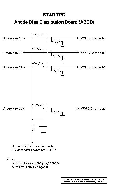
"Anode Bias Distribution Board" (ABDB)
in groups of 20, or from a
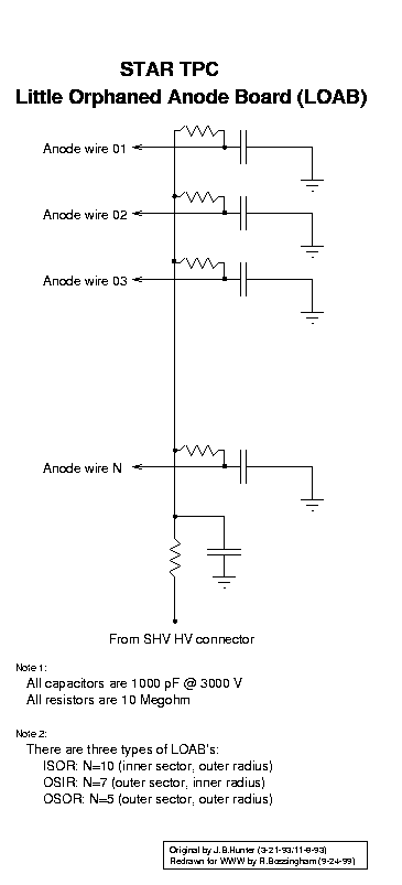
"Little Orphaned Anode Board" (LOAB)
in smaller groups. There are three distinct types of LOAB:
Within each subsector, 160 anode wires, in groups of 20, get HV from ABDB's and send signals to MWC card sockets. Special MWC boards - resembling the FEE cards for the pads - plug into these sockets.
Notes:
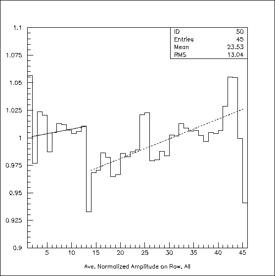
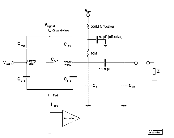
When the ground-wire pulser is used for gain calibration, the response from the inner and outer subsectors differs due to the capacitive coupling between the ground wires and pads. If the MWC cards are powered, all anode wires are AC grounded, and the induced pad-plane signal is reduced uniformly on all pad rows. When the cards are not powered, those anode wires appear to be AC coupled to ground with an impedance of the same order as their coupling to the pulsed ground wires. Therefore, the signals induced on the pad rows vary from row to row, being smallest when the nearby anode wires are coupled to ground through a LOAB, and largest if they are left floating; the effect of the unpowered MWC cards is somewhere in between.
The effect was clearly visible when the pulser data, analyzed by Fabrice Retiere for several sectors of the (then) new electronics, was plotted by row. While not all features in the plot below have been explained, note the following features:
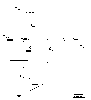
The situation is approximately as represented below, where C_S1 and C_S2 are the small capacitances of the cable, PC board, connector, etc.
This can be simplified with reasonable, AC approximations. The effect of the gating grid and the DC HV circuit are nearly negligible, so we can ignore them. The impedance due to the 1000 pF coupling capacitor is small enough that we can treat it the capacitor as infinite, and combine C_S1 and C_S2 into C_S.
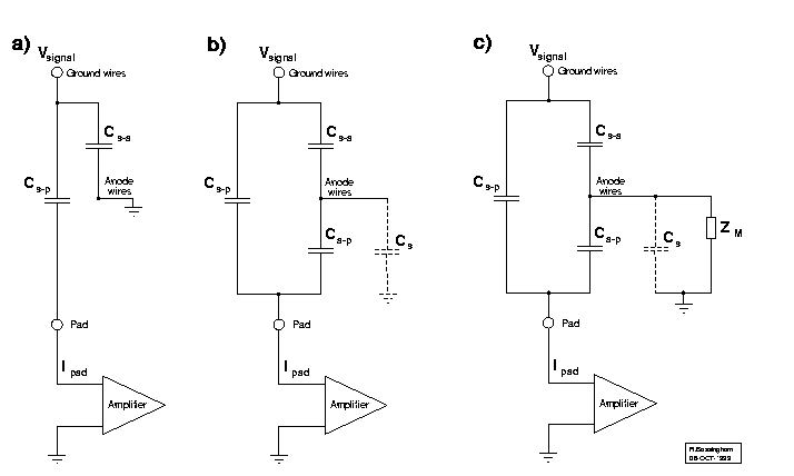
Then, one has one of the three sets of circumstances shown below, depending on the anode wire connections:
Some relevant information follows:
All ABDB and LOAB resistors are 10 megohm; all capacitors are 0.001 uF. HV goes through a resistor to the group of 20 anode wires, then through another resistor to each anode wire. Anode is AC coupled through a capacitor.
On ABDB's, a connection to the MWC socket and a resistor follows the capacitor; on LOAB's, the capactor connects directly to ground.
See the calculated capacitances for the anode, ground and gating-grid wire capacitances.
Thanks to Jim Hunter, Eric Hjort and Jon Wirth for information and prints on the ABDB's, LOAB's and their connections; and to Spencer Klein and Joakim Nystrand for information on the MWC cards.