The FEE readout board address mapping is given below. These addresses
apply to data accessed through either the HDLC link (e.g., by Slow
Controls) or the modem link to the readout board daughter card.
Additional information follows:
-
Housekeeping voltages, temperatures, etc. are in the range -10V to
+10V (read only). The format is 16-bit, bipolar two's complement. All
``voltages'' need a single multiplicative scaling factor to convert to
engineering units (volts). Temperatures need a conversion algorithm
to convert to degrees C :

where
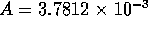 ,
,
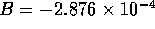 and
and
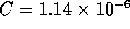 .
.
V is in volts, from -1V to -8V for 0-40C temperatures.
-
The Pulser Amplitude DAC is 12-bit binary read/write, with 0xFFF
corresponding to maximum amplitude. An independent monitor of this
voltage is available thru the ``VDC'' monitor at location 2000E;
max.=-3.5V, min.=-5.00V.
-
Pulser bits are write only. Writing the second (upper) word of a pair
causes all 32 bits to be shifted into the designated FEE card.
-
Each Regulator Control Word uses only the LSB to control the power to
one of nine groups of four FEE cards; these words are read/write.
-
Writing into the Trigger Command Word has the same effect as receiving
that command over the Clock/Trigger cable. A safety bit (211) has
been added. To write a trigger word = 4 and cause an event of type 4
to be generated, for example, write 0x804 into location 20302.
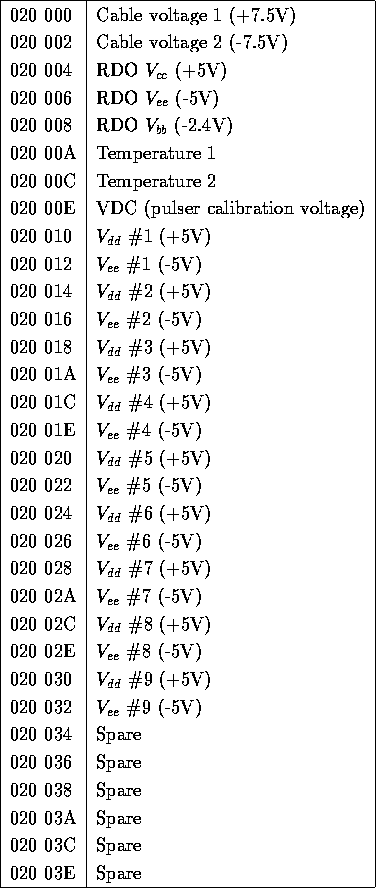
Table 1:
Addresses 020000-0200FE: housekeeping data (read only).
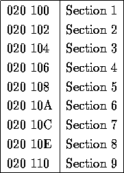
Table 2:
Addresses 020100-0201FE: regulator controls (read/write).
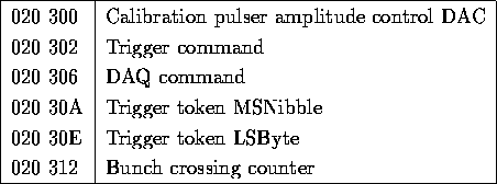
Table 3:
Addresses 020300-0203FE: CSRs, header information.
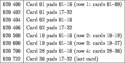
Table 4: Addresses 020400-0207FE: Pulser bits.

Table 5: Addresses 800000-9FFFFE: Event buffer.
Text provided by Fred Bieser (19-NOV-1996)