Last Updated: 15 June 1995
This section gives specifications for the main electronics components associated with the SVT. Table III summarizes the specifications for the on-detector front end electronics.
The charge produced by the passage of ionizing particles through the bulk of
the detectors is collected on segmented anodes, with a pitch of 250 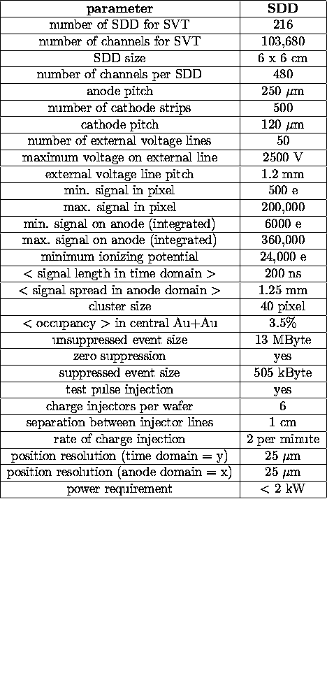 m,
on the far edges of the detector.
The 240 anodes on both ends of the detector are wire-bonded to an
electronics carrier which houses bipolar preamplifier/shaper chips
(PASA) and a CMOS based switch capacitor array (SCA) used as an analog
memory pipeline.
m,
on the far edges of the detector.
The 240 anodes on both ends of the detector are wire-bonded to an
electronics carrier which houses bipolar preamplifier/shaper chips
(PASA) and a CMOS based switch capacitor array (SCA) used as an analog
memory pipeline.
In 300  m of Silicon a minimum ionizing particle traversing at
normal incidence will generate 24,000 electrons. However, diffusion and
Coulomb repulsion limits the signal
in a single electronics pixel to not more than 5,000 electrons.
The incoming signals from the SDD are preamplified and shaped in the
PASA. The intrinsic noise of the readout chain does not exceed 400 rms
electrons, leading to a signal to noise ratio of 60:1. Detector response
simulations show that this ratio is required to achieve excellent position
resolution. The complete readout chain is designed to have a
dynamic range that allows measurement of the energy deposition of minimum
ionizing particles (1 MIP) as well as low momentum (
m of Silicon a minimum ionizing particle traversing at
normal incidence will generate 24,000 electrons. However, diffusion and
Coulomb repulsion limits the signal
in a single electronics pixel to not more than 5,000 electrons.
The incoming signals from the SDD are preamplified and shaped in the
PASA. The intrinsic noise of the readout chain does not exceed 400 rms
electrons, leading to a signal to noise ratio of 60:1. Detector response
simulations show that this ratio is required to achieve excellent position
resolution. The complete readout chain is designed to have a
dynamic range that allows measurement of the energy deposition of minimum
ionizing particles (1 MIP) as well as low momentum ( 100 MeV/c)
protons (
100 MeV/c)
protons ( MIPs).
The shaped signals are stored in a switched capacitor array as a function
of arrival time.
The SCA is clocked at a frequency of 27 MHz and has a depth of 128
time-buckets. It is operated as a circular buffer to avoid the loss of
drift space implied by the 1  s Level-0 trigger delay.
Each PASA and SCA chip hosts 16 channels. The chips will share an on detector Hybrid mounted on a 2 cm wide Beryllia substrate to reduce radiation length on the detector. The inclusion of the SCA on the detector provides multiplexing capabilities leading to a drastic reduction (factor 240) of the number of cables to be attached to the detector and hence not only simplifies the design but allows a reduction of the effective detector mass.
The SCA output is subsequently transmitted to the readout boards (RDO) located at the TPC end caps. Each readout board houses ADCs and a fiber link driver used to send the 10 bit ADC output to the DAQ. Part of the RDO is a power conditioning sector which distributes all required low voltage power levels.
High voltage will be supplied to voltage dividers via separate HV lines. The dividers are located at the water manifolds on each side of the SVT. Each divider board serves 1/2 ladder, which results in 72 lines.

Table: A summary of system requirements for SVT front end electronics