STAR Endcap SMD (MAPMT) Readout Electronics
Last revised Nov. 3, 2005. These documents are for informational purposes only - DO NOT USE THEM FOR ANY DESIGN OR FABRICATION without confirming that you have the most current version.
Questions concerning the MAPMT readout hardware may be directed to Gerard Visser, gvisser "at" indiana.edu.
QUICK PLACEMENT OF DOCUMENTS FOR SLOW CONTROLS DEVELOPMENT - I will organize better later

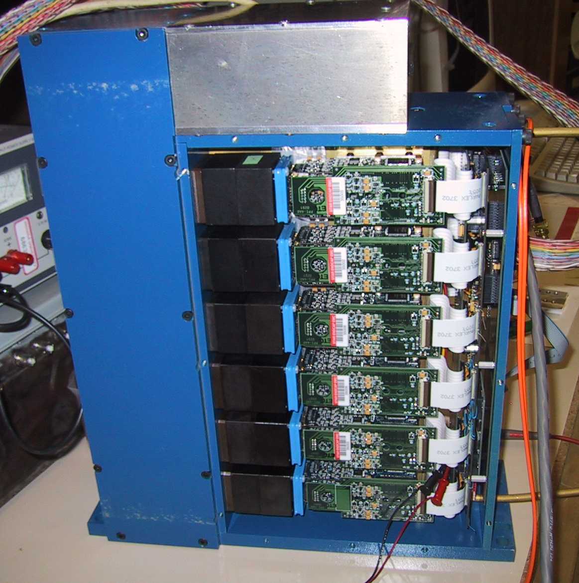
Here is a picture of the complete MAPMT box.
Overview
The front-end electronics for the MAPMT's of the STAR Endcap EMC is mounted directly behind the MAPMT's and CW base assemblies,
inside the same boxes. Forty-eight of these boxes are used for the complete detector, mounted on the back of the poletip. Each
box provides 192 channels of readout.
The 192 channels are divided into twelve modules of 16 channels each (one module per MAPMT). Defective modules may be shut down without interfering with the operation or readout of data from the other modules in the same box (or the other boxes.)
Each MAPMT anode output is directly received by a gated integrator circuit comprised of an AD8039 low-power operational amplifier and a Schottky diode bridge reset circuit. (Kickback from the reset circuit out the input does occur, but settles out quickly enough because of the short direct connection to the MAPMT -- no input buffer is needed.) The integrator outputs are buffered by DC-coupled gain stages; each drives one half of a TSA1204 dual-channel 12-bit pipeline A/D converter. The integrator reset is active for about 22 ns of each RHIC cycle. The duration and phase of the reset with respect to the A/D converter clock are controlled by RC-delay circuits with programmable delay. A third programmable delay circuit allows the phase of the MAPMT box circuitry to be adjusted by up to 60 ns with respect to the RHIC clock. An integration window flat to within 0.1% is achieved with a width of about 45 ns.
Data from the A/D converters is written into circular buffers implemented in a Spartan-II FPGA. When a L0 trigger is received, the appropriate data slice is captured from the buffer (together with pre- and post-event data, when that mode is enabled), formatted, and sent to the Endcap EMC data collector to await a L2 trigger decision.
In addition to the readout functions, the MAPMT box provides housekeeping functions such as a test pulser, temperature, voltage, and current monitors, modular power shutdown, clock and reset timing adjust, and data monitors, under the control of a standard STAR HDLC mezzanine board. The internal test pulser (an independent pulser for each channel) consists of a charge storage capacitor and a MOSFET switch to inject charge from the capacitor directly to the FEE board input connection. The test pulser exercises the full signal and control path with the exception of the MAPMT, CW base, the input connector, and some portions of the trigger/command decoding logic on the readout board. A 12-bit DAC common to all four channels on a FEE board sets the amplitude, controlling precharging of the four test pulser capacitors.
Each MAPMT box is addressed by an HDLC "node address" set by a dipswitch. Channel numbering within the box is hard-wired. The configurations of the FPGA's in the box are stored in a serial flash memory which may be reprogrammed remotely via HDLC. The FPGA's auto-download their configurations from this memory, so no intervention from HDLC is required to start up the box. (Ordinarily, though, there will be parameters such as the reset timing, etc., which have to be set.)
The MAPMT HV system is entirely separate from the readout electronics, merely wired through in the box to a connector on the back panel. It consists of an independent Cockroft-Walton multiplier (running at fixed frequency with current-mode control) for each MAPMT. An external controller supplies the input voltage to the Cockroft-Walton (160 VDC) and controls the operation. Each controller module can handle up to 512 CW bases. See www.hvsys.dubna.ru.
Design documents
Board Schematics (pdf)
Status
(4/30/03) Some slides for FEE design review.
(12/18/02) Old sketch of status (including some specifications).
Results
In November 2002, a single-channel, prototype was constructed on a solid copper ground plane circuit board. The prototype consists of the gated
integrator circuit, a TSA1201 ADC (single-channel version of the TSA1204), and clock and reset signal buffers. Readout of the data is by means
of an HP 1663C logic analyzer (after being captured in 74LCX573 registers). Measurements taken on this circuit verify the general performance
of this design, and will serve as a benchmark for comparison with the production version of the FEE (which has since been fabricated).
On the November prototype, here are results from a near-full-scale test pulse input, showing noise level and the effect of arrival time of the pulse (relative to the RHIC clock). Note the 38 ns time window with response flat to +/- 0.1%. This may be expected to improve slightly by tweaking some resistor and capacitor values (which is not practical in the prototype construction), and by optimizing the reset timing. The improved signal routing, and power and reference bypassing, of the real FEE printed circuit board will likely improve the flatness as well. Furthermore, the test pulse generator does not generate a perfect delta-function of current with respect to time - the width (and overshoot) of the test pulse is responsible for some of the observed deviation from the ideal flat response.
In February 2003 the first real set of boards and real MAPMT box hardware was assembled, together with preliminary control software and readout FPGA logic and the HVSYS Cockroft-Walton bases for the MAPMT's. Early results from LED pulser are reasonable. Note that the apparently poor time response in the first plot is due to the LED pulser circuit. An improved LED drive circuit was contructed, and the time response shown in the last two plots (both plots are of the same data) suggests good performance (with respect to a flat-top integration window) is achieved with this FEE circuit. Results from a capacitor charge injection test circuit are here. This provides a much narrower test pulse, but some of the overshoot and settling errors seen here are artifacts of the test pulser.
(April 16th) The first box is assembled now with three FEE assemblies at locations #6, 7, and 8. Configuration and readout of multiple FEE assemblies is now possible. Installation of the remaining nine FEE assemblies is in progress. Test procedures and analysis software are under development. Here are pedestal means and sigmas from this configuration. Pedestals match to about +/- 10 ADC units rms (0.25 %), which is as expected. (Remember that there are no adjustment knobs for pedestal or gain in this design.)
(May 21st) Internal test pulser results are now available. This will be used for production testing.